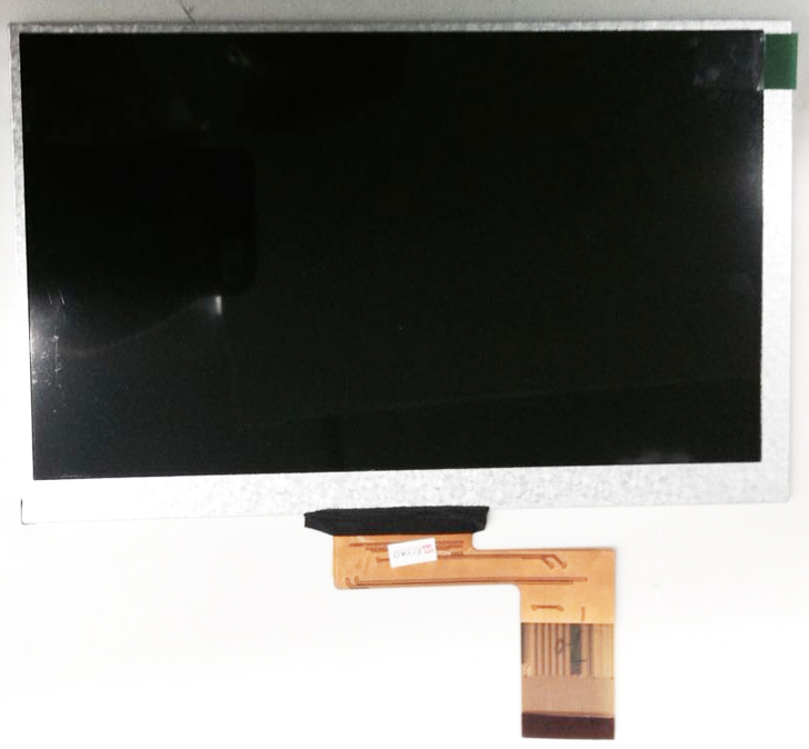
1024*600 LCD screen for FirstSing FS987095 7 inch Dual Core Tablet PC ATM7021 Dual Core With HDMI Android 4.4

SPECIFICATION
LIQUID CRYSTAL DISPLAY MODULE
1.Basic Specifications
1-1 Mechanical specifications:
Items Nominal Dimension Unit
Active screen size 7.0” diagonal -
Dot Matrix 1024 x RGB x 600 Pixel
Module Size ( W×H×T ) mm.
Active Area ( W×H ) 153.6x 90.0 mm.
Pixel Pitch ( W×H ) 0.15x 0.15 mm.
Color depth 16.7M color
Interface LVDS -
Driving IC Package COG -
Module weight 100 g
1-2 Display Specifications:
Display Descriptions Note
LCD Type a-Si TFT -
LCD Mode TN / Normal white -
Polarizer Mode Transmissive -
Polarizer Surface Clear type -
Pixel arrangement RGB-stripe -
Backlight Type LED -
Viewing Direction
(Gray inversion)
6 O‘clock Direction -
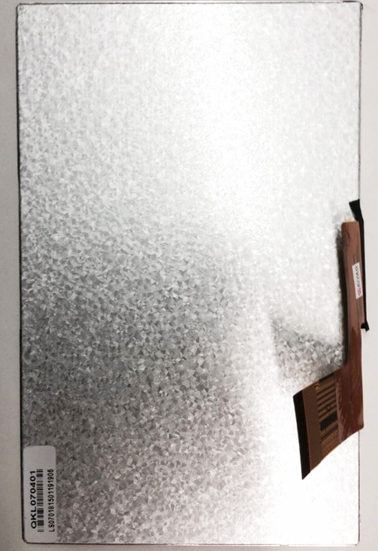
模组成品图:
1-5 Interface Pin Connection:
Pin No. Pin Symbol I/O Description
1 Vcom P Common Voltage
2,3 VDD P Power supply for digital circuit
4 NC - No connection
5 RESET I External reset input, low active
6 STBYB I External standby mode selection, low active
7 GND P Ground
8 RXIN0- I Negative LVDS differential data inputs.
9 RXIN0+ I Positive LVDS differential data inputs.
10 GND P Ground
11 RXIN1- I Negative LVDS differential data inputs.
12 RXIN1+ I Positive LVDS differential data inputs.
13 GND P Ground
14 RXIN2- I Negative LVDS differential data inputs.
15 RXIN2+ I Positive LVDS differential data inputs.
16 GND P Ground
17 RXCLKIN- I Negative LVDS differential clock inputs
18 RXCLKIN+ I Positive LVDS differential clock inputs
19 GND P Ground
20 RXIN3- I Negative LVDS differential data inputs.
21 RXIN3+ I Positive LVDS differential data inputs.
22 GND - Ground
23 NC - No connection
24 NC - No connection
25 GND P Ground
26 NC - No connection
27 DIMO I
Backlight dimmer signal for external controller.
DIMO=H, Logical control signal to turn on external backlight
controller.
DIMO=L, Turn off external backlight controller.
If CABC off, DIMO=DIMI. Else DIMO is controlled by CABC.
1-5 Interface Pin Connection:cont
Pin No. Pin Symbol I/O Description
28 SELB I 6bit/8bit LVDS mode select
29 AVDD P Analog power
30 GND - Ground
31,32 LED- P Power supply for LED Negative
33 L/R I
Source Driver Left or Right sequence control. Normally pull
high.
SHLR=H, Shift to right
SHLR=L, Shift to left
34 U/D I
Gate Driver up/down scan setting. Normally pull low.
UPDN=H, Down to up
UPDN=L, Up to down
35 VGL P Power supply for Gate off output.
36 CABCEN1
37 CABCEN0
I
CABC H/W enable pin. Normally pull low.
CABC_EN=’00’, CABC off.
CABC_EN=’01’, user interface image.
CABC_EN=’10’, still picture.
CAB C_EN=’11’, moving image.
38 NC/VGH -/P No connection/ Power supply for Gate on output.
39,40 LED+ P Power supply for LED Positive
2.Electrical Characteristics
2-1 Absolute Maximum Ratings:
Items Symbol Min. Max. Unit
Input voltage VDD -0.3 4.0 V
Supply Voltage AVDD 6.5 13.5 V
Gate on voltage VGH -0.3 20 V
Gate off voltage VGL -20 0.3 V
Operate temperature range TOP 0 50 ℃
Storage temperature range TST -20 60 ℃
Note1: VDD: Digital I/O Data
Note2: Functional operation should be restricted under ambient temperature (25℃)
Note3: Maximum ratings are those values beyond which damages to the device may
occur. Functional operation should be restricted to the limits in the Electrical
Characteristics chapter.
2.Electrical Characteristics
2-1 Absolute Maximum Ratings:
Items Symbol Min. Typ. Max. Unit Condition
Digital supply voltage VDD 3.0 3.3 3.6 V
Analog supply voltage AVDD 9.4 9.6 9.8 V
Gate on voltage VGH 17 18 19 V
Gate off voltage VGL -6.6 -6 -5.4 V
Vcom voltage VCOM 2.15 2.35 2.55 V Note1
Input high level voltage VI H 0.7VDD - VDD V
Input low level voltage VI L GND - 0.3VDD V
Current for VDD IVDD TBD mA Note2
Current for AVDD IAVDD TBD mA Note2
Current for VGH IVGH TBD mA Note2
Current for VGL IVGL TBD mA Note2
Current for Vcom IVcom TBD mA Note2
Current for VLED ILED 140 mA Note2
Note1:Please adjust VCOM to make the flicker level be minimum.
Note2:The current consumption are under the 25℃, fv=60Hz condition whereas Mosaic
pattern is displayed and fv is the frame frequency.
2-2 DC Characteristics:
2-3 AC Characteristics
2-4 Power on sequence
No. Item Symbol / temp. Min. Typ. Max. Unit
Tr 25
℃
- 5 10
1 Response Time
Tf 25
℃
- 15 30
ms
Θ
2+ 75
Hor.
Θ
2-
75
Θ
1+ 70
2
Viewing
Angle
Ver.
Θ
1-
Center
CR>=10
75
degree
3 Contrast Ratio Cr 25
℃
400 500 - -
Red x-code Rx - 0.57. -
Red y-code Ry - 0.34 -
Green x-code Gx - 0.3 -
Green y-code Gy - 0.57 -
Blue x-code Bx - 0.14 -
Blue y-code By - 0.09 -.
White x-code Wx 0.26 0.31 0.36
White y-code Wy 0.28 0.33 0.38
-
4
Brightness Y
25
℃
- 200 - cd
/㎡
5 Luminance uniformity Yu 25
℃
70 75 - %
3.OPTICAL CHARACTERISTICS
3.1 Characteristics
Electrical and Optical Characteristics